


PCB crosstalk is a common issue in PCB design that can cause signal distortion, noise, and timing errors. It occurs when the electric or magnetic fields generated by one trace interfere with adjacent traces. To ensure reliable communication and proper functioning of electronic devices, PCB designers must carefully manage PCB crosstalk.
This article will explore the issue of crosstalk in pcb boards in detail, including what is PCB crosstalk and its mechanism, why crosstalk occurs and how to reduce PCB crosstalk.
What is PCB crosstalk?

PCB crosstalk refers to board (PCB) interfere with signals on an adjacent trace. This interference is caused by electromagnetic fields that are generated by the current flowing through the traces. The fields can induce voltages in nearby traces, leading to unwanted noise and distortion in the signals.
The severity of PCB crosstalk is effected by the distance between the PCB traces, the frequency of the signals, and the characteristics of the traces themselves. Therefore, from PCB layout design to PCB manufacturing to PCB assembly, PCB manufacturers should think about how to reduce PCB crosstalk and provide customers with high-quality and high-performance products.
Crosstalk in PCB
In PCB design, crosstalk refers to the unwanted electromagnetic coupling between adjacent traces on the board. When signals are transmitted through traces, they generate electromagnetic fields that can cause nearby traces to pick up some of the signal’s energy. This interference can result in signal distortion, noise, or other undesirable effects that can degrade the performance of the circuit.
PCB crosstalk can occur in both digital and analog circuits, and can be influenced by factors such as the distance between the traces, their orientation, the frequencies of the signals, and the materials used in the board’s construction. PCB designers and PCB manufacturers must carefully manage crosstalk to ensure that circuits operate as intended and avoid PCB signal integrity issues.
Crosstalk mechanism

1. Coupling: PCB crosstalk occurs due to the coupling of electromagnetic fields generated by the signals transmitted through adjacent traces. When a signal passes through a trace, it creates an electric field that can induce a voltage in nearby traces, even those that are not directly connected to it. This phenomenon is known as capacitive coupling. The amount of coupling depends on the distance between the traces, their orientation, and the characteristics of the signals themselves. Inductive coupling can also occur when a changing current in one trace induces a voltage in an adjacent trace.
This mechanism is influenced by the distance between the traces, the frequency of the signals, and the orientation of the traces with respect to each other. The result of these coupling mechanisms is that signals on one trace can interfere with signals on adjacent traces, leading to crosstalk and potentially degrading the performance of the circuit. To minimize crosstalk, PCB designers may use techniques such as careful trace routing, ground planes, and shielding to manage the coupling between traces.
2. Signal or line switching: Two parallel lines in the PCB, when one of them has a high-speed signal transmission, generate an alternating magnetic field, after acting on the other line, generates an induced current inside the line. Now the integration of electronic products is getting more and more high, the packaging is getting smaller and smaller, the PCB trace is getting more and more dense, PCB crosstalk is a particularly difficult to predict and control the phenomenon, inevitable, also cannot be eliminated, can only be reduced as far as possible.
What causes PCB crosstalk?
- Capacitive coupling and inductive coupling: PCB crosstalk is caused by the coupling of electromagnetic fields generated by signals transmitted through adjacent traces on the board. When a signal passes through a trace, it generates an electric field that can induce a voltage in nearby traces, even those that are not directly connected to it. This is known as capacitive coupling. Inductive coupling can also occur when a changing current in one trace induces a voltage in an adjacent trace.
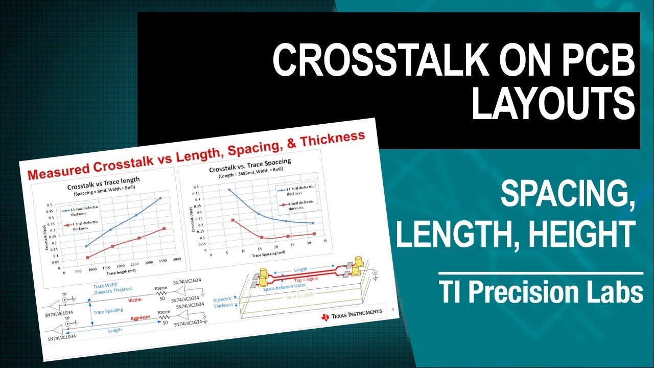
- Line spacing: The closer the distance between signal paths, the more obvious the crosstalk will be. As the line spacing increases, both the near-end and far-end crosstalk will decrease.
- The degree of signal change: the instantaneous change of signal will bring obvious magnetic field effect. The steeper the rising/falling edge of the signal, the more obvious the crosstalk. Similarly, the different speeds of signal propagation in the PCB will also cause PCB crosstalk.
- PCB size and thickness: The dielectric thickness here refers to the distance from the signal to the reference layer. Variations in PCB substrate thickness can cause variations in crosstalk. In general, the smaller the thickness of the dielectric layer, the smaller the crosstalk. Also, as the size of the PCB board increases, the length of the traces will also increase, thereby increasing the possibility of PCB crosstalk.
- PCB vias: PCB vias with stubs will generate reflections, which is also one of the causes of PCB crosstalk.

What are the different types of crosstalk in PCB?
The two main types of crosstalk in PCBs are capacitive crosstalk and inductive crosstalk.
Capacitive crosstalk: Capacitive crosstalk occurs when the electric field generated by a signal in one trace induces a voltage in an adjacent trace
Inductive crosstalk: Inductive crosstalk occurs when a changing current in one trace induces a voltage in an adjacent trace.
Both types of crosstalk can cause unwanted interference between signals and degrade the performance of the circuit. PCB designers must carefully manage these types of crosstalk through proper trace routing, spacing, and shielding techniques to ensure reliable communication and proper functioning of the electronic device.
What are the effects of crosstalk on PCB?
Crosstalk may be the most important influencing factor in high-speed data transmission, and it may cause data transmission loss and transmission errors. So crosstalk is the biggest natural enemy for PCB design and PCB layout.
The effects of crosstalk on PCB can also include signal distortion, noise, and timing errors. Crosstalk can cause unwanted interference between signals, leading to a reduction in the signal-to-noise ratio, which can degrade the performance of the circuit. In digital circuits, crosstalk can cause errors in data transmission and lead to timing violations, while in analog circuits, it can cause
distortion and affect the accuracy of measurements. Managing crosstalk is important to maintain signal integrity and ensure proper functioning of the electronic device.
How to reduce PCB crosstalk?

To reduce crosstalk in PCB design, several techniques can be used, including:
1. Line track spacing and impedance: appropriately increase the spacing between signal paths; reduce the characteristic impedance of the signal path
2. Return path: Use a plane as the return path;
3. Routing design: Optional routing at the strip line layer; use guard routing with short-circuit via at both ends and across the entire line.
4. PCB selection: use a stack with a lower dielectric constant;
5. Package and Connector: Do not share return pins in package and connector
6. Shielding: During PCB design, a shielding layer can be added between sensitive traces to reduce electromagnetic interference and crosstalk.
7. Termination: Adding a termination resistor at the end of the trace can reduce reflections and signal ringing, thereby reducing crosstalk.
8. Signal lines: Sensitive signal lines, such as audio and other analog signals, should be kept away from digital signal lines as far as possible, and should not be paralleled with digital signal lines; key high-speed signal lines should be wrapped with GND as much as possible.
9. PCB crosstalk analysis: Performing crosstalk analysis during the design process can help identify potential crosstalk issues and allow for adjustments to be made to minimize their effects.
By implementing these techniques, PCB designers can reduce crosstalk and maintain signal integrity, ensuring proper functioning of the electronic device.
How to calculate PCB crosstalk?

Calculating crosstalk in a printed circuit board (PCB) can be a complex process that depends on various factors such as trace length, distance between traces, trace width, and signal frequency. One approach to estimating crosstalk is to use a crosstalk calculator, which is a software tool that can simulate the coupling between traces and predict the level of crosstalk based on input parameters.
To use a crosstalk calculator, you typically need to provide the following information:
1. The distance between the traces
2. The trace length
3. The trace width (PCB trace width calculator)
4. The thickness of the dielectric layer between the traces
5. The dielectric constant of the PCB substrate material
6. The signal frequency and edge rate
7. The type of coupling (capacitive or inductive)
Based on this information, the calculator can estimate the amount of crosstalk between the traces and provide guidance on how to minimize it through adjustments such as trace spacing, routing, and termination.
It’s important to note that while crosstalk calculators can provide valuable insights, they are not always accurate, and the actual crosstalk in a PCB can be affected by other factors not accounted for in the calculations. Therefore, it’s essential to use crosstalk calculations as a guide and to perform crosstalk analysis and testing to ensure the proper functioning of the circuit.
Conclusion
In summary, reducing crosstalk in PCB design requires a combination of proper trace routing, spacing, and shielding techniques, along with crosstalk analysis and testing. By minimizing the interference between traces, PCB designers can maintain signal integrity and ensure the optimal performance of electronic devices.
As a professional ODM service provider, IBE provides solutions integrating design, manufacturing and assembly for electronic products in the fields of automotive electronics, industrial control, medical beauty, sports entertainment, etc., always adheres to the strictest product quality control to ensure the good operation of the product, and constantly explore new solutions to meet the product needs of the society and customers.
There are several reasons that may cause crosstalk:
1. Capacitive coupling and inductive coupling
2. Close line distance
3. Different speeds of signal change and propagation
4. PCB size and thickness: too big and too thick
5. PCB vias
1. Appropriate line track spacing and impedance
2. Use a plane as the return path
3. Routing design
4. Use a stack with a lower dielectric constant
5. Do not share return pins in package and connector
6.Routing design: Optional routing at the strip line layer; use guard routing with short-circuit via at both ends and across the entire line.
Preventing crosstalk in PCB (Printed Circuit Board) designs is crucial for maintaining signal integrity and overall performance.
Increase Trace Spacing: Ensure adequate spacing between signal traces, especially those carrying high-speed or sensitive signals. Greater distances reduce the likelihood of interference.
Use Ground Planes: Incorporate solid ground planes in your design. These act as shields that absorb and dissipate electromagnetic interference, helping to isolate signal traces and reduce crosstalk.
Implement Differential Pair Routing: For high-speed signals, use differential pairs with closely coupled traces. This technique improves noise immunity and minimizes crosstalk by ensuring that any interference affects both lines equally.
Route Traces Perpendicularly: Avoid running high-speed signal traces parallel to each other for long distances. If parallel routing is necessary, ensure it is kept to a minimum and use perpendicular crossings where possible.
Use Proper Trace Widths and Impedance Control: Match trace widths and control impedance to suit the signal frequency. This helps maintain signal integrity and reduces potential for crosstalk.
Add Shielding: Use trace shielding techniques, such as placing a ground trace or plane between signal traces, to create a barrier that reduces crosstalk.
Design with Decoupling Capacitors: Place decoupling capacitors near sensitive components to filter out noise and stabilize power supplies, which can help minimize signal interference.
Run Sensitive Signals Separately: Isolate critical or sensitive signal lines from high-power or high-speed lines to prevent interference.
By incorporating these techniques into your PCB design, you can effectively reduce crosstalk, ensuring cleaner signals and improved performance of your electronic devices.
The rule of thumb for managing crosstalk in PCB (Printed Circuit Board) design is to maximize the distance between signal traces carrying high-frequency or sensitive signals.
Increase Trace Separation: Keep high-speed or critical signal traces as far apart as practical. Greater spacing reduces the potential for electromagnetic interference between traces.
Use Ground Planes: Incorporate continuous ground planes to act as shields. They help absorb and block noise, preventing it from affecting adjacent signal lines.
Avoid Parallel Routing: Minimize parallel routing of high-speed traces. If parallel routing is necessary, ensure it's limited and use ground traces or planes between them.
Implement Differential Pairs: For high-speed signals, use differential pairs where two closely spaced traces carry the signal. This configuration improves noise immunity and reduces crosstalk.
Maintain Proper Trace Widths and Impedance: Ensure trace widths and impedance are correctly matched to the signal frequencies to maintain signal integrity and reduce potential interference.
The "3W rule" for crosstalk in PCB design is a guideline to help minimize signal interference between traces. It stands for:
Width: Maintain a sufficient distance between parallel signal traces to reduce crosstalk. The wider the spacing, the lower the potential for interference. Typically, the spacing should be at least three times the trace width, but this can vary based on the specific design and signal frequency.
Wave: Focus on the signal's wavelength. High-frequency signals have shorter wavelengths, making them more susceptible to crosstalk. Ensure that critical traces are routed to minimize coupling over their wavelength, which often involves increasing spacing or using shielding.
Way: Route sensitive or high-speed signals away from noisy or high-power traces. By strategically planning the layout to avoid parallel runs and using appropriate routing techniques, you can further reduce crosstalk.
Following the 3W rule helps in designing PCBs with better signal integrity by addressing trace spacing, wavelength considerations, and routing practices.
- An ultimate introduction to high speed PCB and is it same as high frequency PCB ?
- What is high speed PCB design – guidelines and best practice tips
- Signal crosstalk in chiplet packaging – how to reduce its impact?
- Top 10 best and free PCB layout design software in 2023
- Top 10 PCB assembly manufacturers in the world
- Top 10 HDI PCB manufacturers in the world in 2023
Last updated on August 23rd, 2024 at 07:30 am